
Silicon Evolution via SoIC Vertical Integration
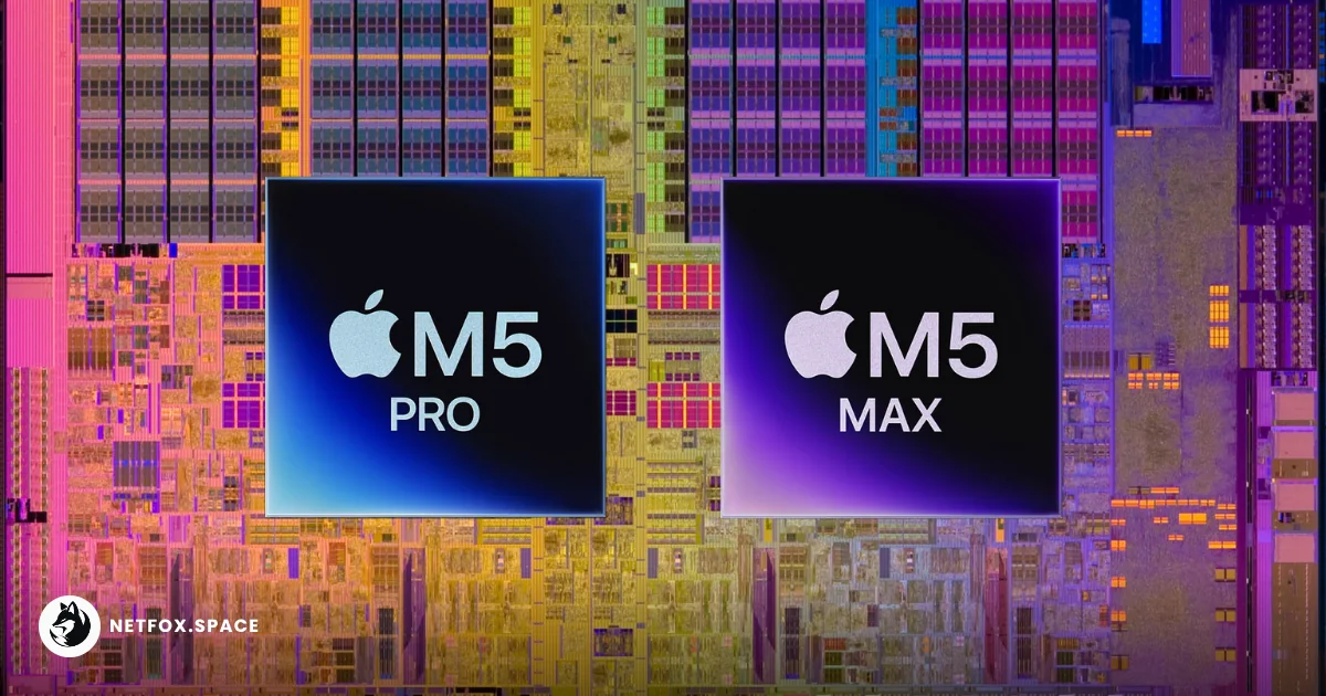
Apple’s upcoming M5 Pro and M5 Max processors are set to depart from traditional monolithic or 2D lateral layouts. According to insights from members of Apple’s Platform Architecture team, the next generation of high-end Apple Silicon will utilize vertically stacked dies. This transition leverages advanced packaging techniques, likely TSMC’s System on Integrated Chips (SoIC) technology, to mimic 3D structural density.
By stacking components vertically rather than spreading them across a horizontal substrate, Apple Inc. can significantly reduce the distance data must travel between the CPU, GPU, and cache. This architecture minimizes latency and heat generation while allowing for a massive increase in transistor density within the same footprint used by the current M4 series.
 The new Apple Mac configurator brings flexibility and granularity to the front.
Thermal Density and Power Delivery Challenges
The move to 3D packaging introduces a shift in how the semiconductor industry manages thermal envelopes. In a vertically stacked environment, the bottom dies are shielded by the top layers, creating a "heat trap" effect that traditional air-cooling methods struggle to resolve. Apple is expected to counter this by implementing high-thermal-conductivity materials and refined power gating.
The M5 Max is specifically rumored to utilize these stacked dies to expand memory bandwidth. By placing the memory controller or specialized SRAM cache layers directly atop the logic dies, Apple can bypass the physical limitations of the UltraFusion interconnect seen in "Ultra" designated chips, providing "Pro" and "Max" users with unprecedented throughput.
The Hybrid Bonding Advantage Over Traditional Interconnects
While competitors often rely on micro-bumps for chiplet connectivity, Apple is reportedly eyeing hybrid bonding for the M5 cycle. This method eliminates the need for solder bumps, using direct copper-to-copper connections between stacked layers.
| Feature | Traditional Flip-Chip Packaging | 3D Hybrid Bonding (M5 Expected) |
|---|---|---|
| Interconnect Pitch | 40–100 microns | <10 microns |
| Data Transfer Rate | Standard | Up to 10x higher density |
| Thermal Efficiency | Moderate | Superior (via direct contact) |
| Z-Height | Thicker | Ultra-slim profile |
This technical shift is not merely an incremental speed boost; it is a structural necessity. As TSMC moves toward 2nm processes, the physical "real estate" on a single wafer becomes too expensive to waste on lateral expansion. Hybrid bonding allows Apple to reclaim vertical space, effectively turning the processor into a high-rise city of transistors.
 Apple/CNET
Shifting the Competitive Landscape of High-End Computing
This architectural pivot places Apple in direct confrontation with Intel Corporation’s Foveros technology and AMD’s 3D V-Cache. However, Apple’s advantage lies in its vertical integration of the operating system and hardware. By controlling the macOS kernel, Apple can optimize thread scheduling specifically for 3D-stacked topologies, ensuring that heat-sensitive tasks are not routed to the bottom layers of the silicon stack.
The implications for the biotech sector and AI research are substantial. The increased memory-on-die capacity afforded by 3D stacking will allow for larger Large Language Models (LLMs) to run locally on MacBook Pro hardware without relying on external GPU clusters. This effectively moves "datacenter-grade" architecture into a portable form factor.
Supply Chain Constraints and Yield Risks
The transition to 3D packaging is fraught with manufacturing complexity that could impact initial availability. Stacking dies requires a "Known Good Die" (KGD) strategy; if one layer in the stack is defective, the entire multi-die assembly potentially costing hundreds of dollars must be discarded. This puts immense pressure on Taiwan Semiconductor Manufacturing Company (TSMC) to maintain near-perfect yields during the M5 production ramp.
Furthermore, the sophisticated nature of SoIC packaging is currently a bottleneck in the global supply chain. If Apple monopolizes TSMC’s 3D packaging capacity for the consumer electronics market, it may force other fabless semiconductor firms to delay their own 3D roadmaps. This creates a regulatory and economic tension where Apple’s architectural leap could inadvertently stifle innovation in secondary markets dependent on the same advanced packaging facilities.
Comments (0)
Please login to comment
Sign in to share your thoughts and connect with the community
Loading...